Cookies on the OMEGA websites We use cookies on this website, these cookies are essential for the website to work correctly.If you continue without changing your settings, we'll assume that you are happy to receive all cookies on this website.To find out more information about these cookies please click here.
The OMB-DAQTEMP series has been discontinued. Please see the OMB-DAQ-TC-RACK as a possible alternative or contact our Application Engineering department for details.
The OMB-DAQTEMP-14A data
acquisition card provides a total
hardware/software/signal
conditioning solution for highaccuracy,
high speed temperature,
voltage, frequency, and pulse
counting measurements, plus digital
I/O and analog output.
A diversified software is included
with the OMB-DAQTEMP-14A, including
DaqView software, plus drivers for
DASYLab, LabView, and Windowsbased
languages including Visual
Basic and C++.
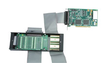
OMB-DAQTEMP-14A hardware is
comprised of a plug-n-play PCI
board, 3 ft cable, and a screw
terminal/signal conditioning pod.
Cold-junction compensation is
built-in to the OMB-DAQTEMP-14A,
providing highly accurate
thermocouple measurements, with
channel-to-channel variation and
noise typically less than 0.2°C,
and absolute accuracy typically
better than 1.0°C.
This is
accomplished by having a separate
low-noise, bandwidth-limited
amplifier per thermocouple channel.
OMB-DAQTEMP-14A provides
14 thermocouple input
channels. All power for the
OMB-DAQTEMP-14A is derived from the
PC, so there is no need for external
power supplies or transformers.
In addition to thermocouple inputs,
OMB-DAQTEMP-14A also provides 7
differential voltage input channels,
with 16 bit resolution and
programmable full scale input
ranges from +156 mV to +10 V.
The 4 frequency input channels can
measure frequency or count pulses
up to 10 MHz. Two timer output
channels are capable of generating
square outputs up to 1 MHz.
Twenty four digital I/O lines are also
included, which can be programmed
in 8 bit groups as either inputs or
outputs.
The 16 bit/100K Hz analog
outputs can be used to generate
waveforms, with a virtually infinite
waveform output length possible
from PC memory.
All inputs and outputs are accessed
via convenient screw terminals
located on the signal conditioning
pod. The cover of the signal
conditioning pod is easily removable
to gain access the screw terminals
for signal connections.
DAQVIEW SOFTWARE
The included DaqView software
allows you to verify signal
connections, acquire and save data
to disk, and graphically view realtime
data within moments of taking
your installing your system. Easily
set up all your hardware,
acquisition, and display parameters,
without programming, via a simple
spreadsheet-style screen. DaqView
is a full featured acquisition and
display application that provides all
the functionality you’ll need for
many datalogging applications.
SWD-DAQVIEW-XL
DaqViewXL is an optional Excel
add-in that provides complete data
acquisition functionality. Seamlessly
integrated into Excel’s tool palette,
DaqViewXL provides you with the
same comprehensive acquisition
and display capabilities as
DaqView. Excel is an ideal tool for
test engineers because it provides a
variety of graph and charting
functions for presenting data in a
graphical format, as well as
mathematical and analysis functions
such as FFTs. Excel’s ability to
retrieve and manipulate previously
acquired data in a spreadsheet
format and DaqViewXL’s advanced
data acquisition functions form a
comprehensive data acquisition
solution.
Specifications
GENERAL Supply Voltage Range: 4.75 Vdc to 5.25 Vdc (from PCI Bus) Power Consumption: 5.5 W Operating Temperature: 0 to 60°C (32 to 140°F) Storage Temperature: 40 to 80°C (-40 to 176°F) Relative Humidity: 0 to 95%, non-condensing Vibration: MIL STD 810E PCI Board Dimensions: 165 W x 15 D x 108 mm H (6.5 x 0.6 x 4.2") Signal Conditioning/Screw Terminal Pod Dimensions:
86 W x 240 D x 42 mm H 3.4 x 9.44 x 1.65")
VOLTAGE INPUTS
Channels: 7 differential inputs, programmable on a per-channel
basis for unipolar or bipolar Ranges: Software or sequencer selectable on a per-channel basis;
0 to10 V, 0 to 5 V, 0 to 2.5 V, 0 to1.25 V, 0 to 0.625 V, 0 to 0.3125 V, ±10 V, ±5 V,
±2.5 V, ±1.25 V, ±0.625 V, ±0.3125 V, ±0.156 V Voltage Accuracy: One year, 0 to 35°C (exclusive of noise); for full-scale input ranges from 2.5 V to
10V, accuracy is 0.015% of reading +0.005% of range. For full-scale input ranges from 312 mV to 1.25 V, accuracy is 0.015% of reading +0.008% of range.
For full-scale input of 156 mV, accuracy is 0.02% of reading +0.008% of range. Bandwidth: 500 kHz Settling Time: 5 us to 1 LSB for full-scale step Temperature Coefficient: ±(10ppm +0.3 LSB)/°C Input Impedance: 20M Ohm
(differential) Bias Current: <1nA (0 to 35°C) Common Mode Rejection: 86 dB, DC to 60 Hz for gains <=8;>100 dB for gains >=16 Maximum Input Voltage: ±11V relative to analog common Over-Voltage Protection: ±35V Crosstalk: 100 dB DC to 60 Hz;
86 dB @10 kHz
THERMOCOUPLE INPUTS
Channels: 14 differential TC inputs TC Types: J,K,S,T,E,B R,N,
or mV input Input Voltage Range: ±100 mV Input Impedance: 40 M . Input Bandwidth: 4 Hz Input Bias Current: 10 nA CMRR: 100dB typ Over Voltage Protection: ±40 V Voltage Accuracy: ±(0.2%of rdg +50 µV) TC Accuracy: See PDF
Valid for one year,18°C to 28°C. Minimum TC resolution: 0.1 °C for all TC types
INPUT SEQUENCER
Temperature,voltage,digital and
frequency inputs can be scanned
synchronously,based on either an
internal programmable timer,or an
external clock source.Analog and
digital outputs can be synchronized
to either of these clocks.
Scan Clock Sources: 2 1. Internal,programmable from
5 µs to 5.96 hours in 5 us steps 2. External,TTL level input up to
200 kHz max
External Acquisition Scan
Clock Input Maximum Rate: 200 kHz Clock Signal Range: 0 to 5 V Minimum Pulse Width: 50 ns high, 50 ns low
TRIGGERING
Trigger Sources: 6,individually
selectable for starting and stopping
an acquisition.Stop acquisition can
occur on a different channel than
start acquisition;stop acquisition can
be triggered via modes 2,4,5 or 6
described below.Pre-trigger is
supported with fixed or variable
pre-trigger periods.
1.Single-Channel Analog
Hardware Trigger
Any voltage or TC input channel
can be software programmed
to be the analog trigger channel
Input Signal Range: -10 to 10 V max Trigger Level: Programmable (11-bit resolution) Hysteresis: Programmable (11-bit resolution) Latency: 5 us max
2. Single-Channel Analog
Software Trigger
Any voltage or TC input channel can
be selected as the software trigger
channel.If the trigger channel is a
thermocouple,then the driver
automatically compensates for the
delay required to obtain the reading,
resulting in a maximum latency of
one scan period.
3. Single-Channel Digital Trigger
A separate digital input is provided
for digital triggering Input Signal Range: -15 to 15 V Trigger Level: TTL
Min Pulse Width: 50 ns high,50 ns low Latency: 5 us max
4. Digital Pattern Triggering
8-or 16-bit pattern triggering on the
digital input port.Programmable for
trigger on equal, above, below, or
within/outside of a window.
Individual bits can be masked for
I don ’t care condition Latency: One scan period max
5. Counter/Totalizer Triggering
Counter/totalizer inputs can trigger
an acquisition.User can select to
trigger on a frequency or on total
counts that are equal,above,below,
or within/outside of a window Latency: One scan period, max.
6. Software Triggering
Trigger can be initiated under
program control
ANALOG OUTPUT
Up to four analog output channels
can be updated synchronously
relative to scanned inputs,and
clocked from either an internal
onboard clock,or an external clock
source.Analog outputs can also be
updated asynchronously,independent
of any other scanning in the system
Channels: 4 Resolution: 16 bits Output Voltage Range: ±10 V Output Current: ±10 mA Offset Error: ±0.0045 V max Gain Error: ±0.01% Update Rate: 100 kHz max, 1.5 Hz min (no minimum with
external clock) Settling Time: 10 us max to 1 LSB for full-scale step Clock Sources: 4, programmable 1. Onboard D/A clock,independent
of scanning input clock 2. Onboard scanning input clock 3. External D/A input clock, independent of external scanning
input clock 4. External scanning input clock
FREQUENCY/PULSE COUNTERS
Counter inputs can be scanned
synchronously along with voltage,
TC and digital scanned inputs,based
either on internal programmable
timer,or an external clock source.
Counters can be configured to clear
when read,or to totalize and clear
under program control
Channels: 4 x 16-bit; cascadable as 2 x 32-bit Frequency Measurement Rate: 10 MHz max Input Signal Range: -15 to 15 V Trigger Level:TTL Minimum Pulse Width: 50 ns high, 50 ns low Frequency/Pulse Generators
Channels: 2 x 16-bit Output Waveform: Square wave Output Rate: 1 MHz base rate
divided by 1 to 65535
(programmable) High-Level
Output Voltage:
2.0 V min @-3.75 mA;
3.0 V min @-2.5 mA Low-Level
Output Voltage:
0.4 V max @2.5 mA
DIGITAL I/O
Channels: 24 I/O Levels: TTL
† All amounts shown in EUR, GBP, or USD Note: All OMB-DAQTEMP14A systems include PCI measurement board, 0.9 m (3')cable, signal conditioning pod, documentation is included on the CD ROM supplied with the system. Additional I/O provided with every system inputs, 24 digital I/O, 4 counter inputs, 2 timer outputs and 4 analog outputs. Software included with the OMB-DaqView, Windows drivers for Visual Basic and C++, and drivers for LabView and DASYLab.
We noticed you are from the US. Visit your local site for regional offers and live support.